Primary Side Regulation(PSR) CV/CC Controller
| ̇Description WIS8801 is a low cost and high performance Primary Side Regulation (PSR) controller for offline small power converter applications which can provide very tight output voltage regulation (CV) and output current control (CC) ideal for charging applications. In CV mode, WIS8801 adopts Muliti Mode Control which uses the hybrid of AM (Amplitude Modulation) mode and (Frequency Modulation) FM mode to improve system efficiency and reliability. In CC mode, the IC use PFM control with line and load CC compensation. The IC can achieve audio noise free operation and optimized dynamic response. The built-in Cable Drop Compensation (CDC) function can provide excellent CV performance. WIS8801 integrates functions and protections of Under Voltage Lockout (UVLO), VDD over Voltage Protection (VDD OVP),Cycle-by-cycle Current Limiting (OCP),Short Load Protection (SLP), Pin Floating Protection, VDD Clamping, etc. |
|||||||||||||||||||||||||||||
| ̇Applications • Battery Chargers for Cellular Phones • AC/DC Power Adapter and LED Drivers • PSR Application:230VAC:7.5W & 85-265VAC :5.5W |
|||||||||||||||||||||||||||||
̇Package Information |
|||||||||||||||||||||||||||||
| ̇Features • Driver Integrated With 700V BJT Driver • Multi Mode PSR Control • Audio Noise Free Operation for PSR • Optimized Dynamic Response for PSR • Low Standby Power <70mW • ±4% CC and CV Regulation • Programmable Cable Drop Compensation:(CDC) in CV Mode • Built-in AC Line & Load CC Compensation • Build in Protections: Short Load Protection (SLP) Cycle-by-Cycle Current Limiting VDD OVP & UVP & Clamp Leading Edge Blanking (LEB) Pin Floating Protection VDD OVP & Clamp • Package:SOP-8 |
|||||||||||||||||||||||||||||
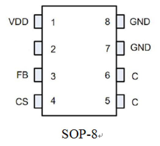
| ̇Pin Configuration | |||||||||||||||||||||||||||||
|
|||||||||||||||||||||||||||||
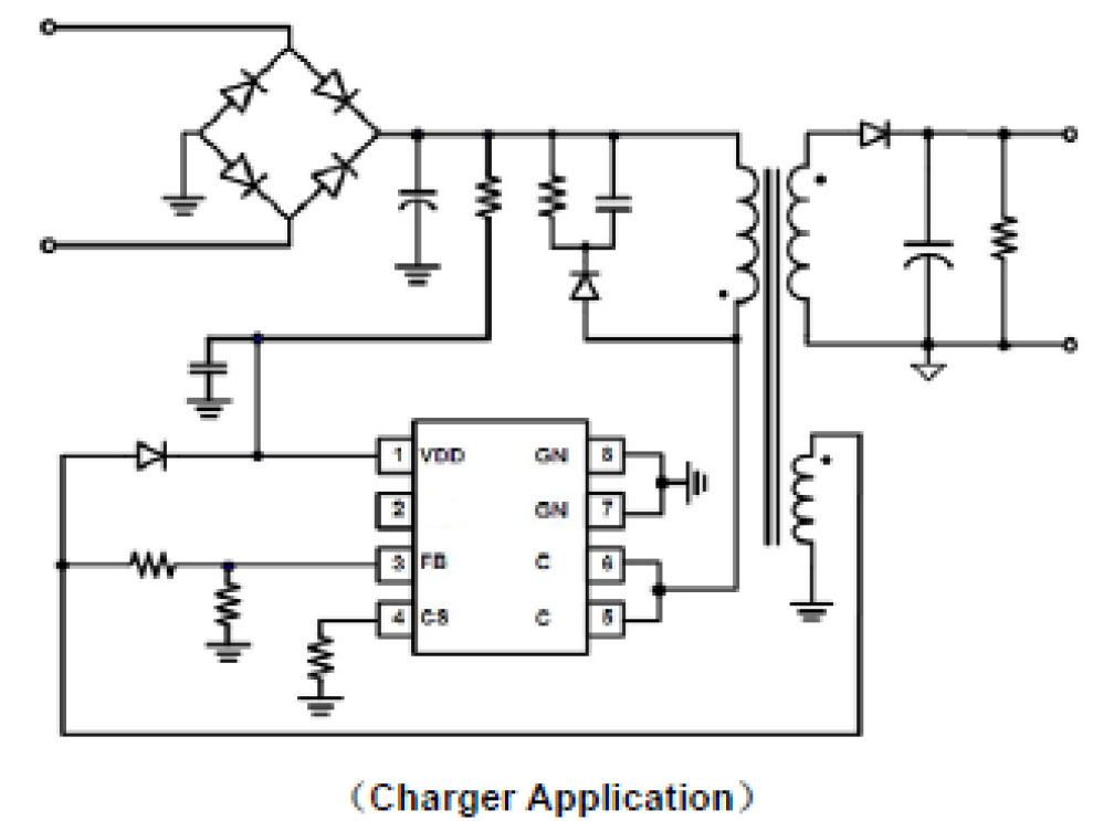
| ̇Typical Application Circuit |
|||||||||||||||||||||||||||||
 |
|||||||||||||||||||||||||||||
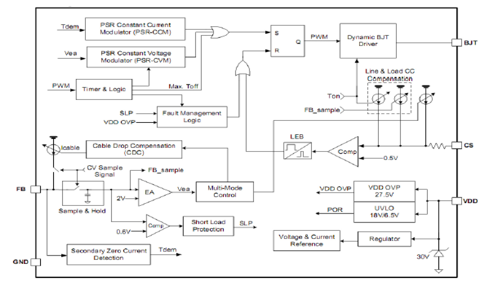
| ̇Block Diagram | |||||||||||||||||||||||||||||
 |
|||||||||||||||||||||||||||||
| WIS8802 Driver IC Multi-Mode Primary Side Regulation(PSR) Power Switch |
|||||||||||||||||||||||||||||
| ̇Description WIS8802 is a family of a high performance Primary Side Regulation (PSR) power switch with high precision CV/CC control ideal for charger applications. The IC can also support Qasi-Resonant(QR) Buck constant current topology for LED lighting if SEL pin is short to GND. In CV mode,WIS8802 adopts Multi Mode Control which uses the hybrid of AM (Amplitude Modulation) mode and (Frequency Modulation) FM mode to improve system efficiency and reliability. In CC mode, the IC uses PFM control with line and load CC compensation. The IC can achieve audio noise free operation and optimized dynamic response. The built-in Cable Drop Compensation (CDC) function can provide excellent CV performance.WIS8802 integrates functions and protections of Under Voltage Lockout (UVLO), VDD over Voltage Protection (VDD OVP), Cycle-by-cycle Current Limiting (OCP),Short Load Protection (SLP), and VDD Clamping. WIS8802 are available in SOP-8 respectively. |
|||||||||||||||||||||||||||||
| ̇Applications • Battery Chargers for Cellular Phones • AC/DC Power Adapter and LED Drivers • PSR Application:230VAC:7.5W & 85-265VAC :5.5W |
|||||||||||||||||||||||||||||
| ̇Package Information | |||||||||||||||||||||||||||||
 |
|||||||||||||||||||||||||||||
| ̇Features • Driver Integrated With 600V MOS • Support Flyback and Buck Topology: Flyback PSR Control(SEL=Floating) QR-Buck CC Control(SEL=GND) • Multi Mode PSR Control • Audio Noise Free Operation for PSR • Optimized Dynamic Response for PSR • Low Standby Power <70mW • ±4% CC and CV Regulation • Programmable Cable Drop Compensation:(CDC) in CV Mode • Built-in AC Line & Load CC Compensation • Build in Protections: Short Load Protection (SLP) On-Chip Thermal Shutdown(OTP) Cycle-by-Cycle Current Limiting Leading Edge Blanking (LEB) Pin Floating Protection • VDD OVP & Clamp • Package:SOP-8 |
|||||||||||||||||||||||||||||
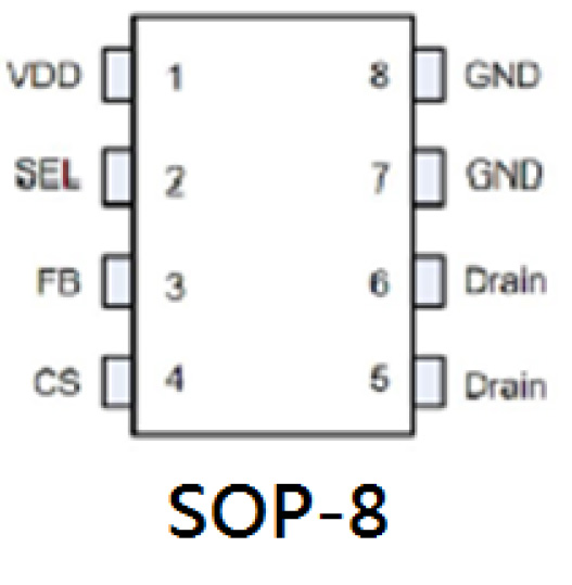
| ̇Pin Configuration | |||||||||||||||||||||||||||||
|
|||||||||||||||||||||||||||||
| ̇Typical Application Circuit | |||||||||||||||||||||||||||||
 |
|||||||||||||||||||||||||||||
| ̇Block Diagram | |||||||||||||||||||||||||||||
 |
|||||||||||||||||||||||||||||